Nor Gate Schematic In Cadence
Cadence virtuoso tutorial: nor gate schematic, symbol and layout Nand xor logic nor vhdl xnor wiring simulate verify circuits scosche input inputs engineersgarage Nor gate gates universal part symbol truth table
Cadence Virtuoso Tutorial: NOR Gate Schematic, Symbol and Layout - YouTube
Lab 03 cmos inverter and nand gates with cadence schematic composer Solved how would i draw a 3-input nor gate using dynamic Xor logic gate circuit diagram : 1
Nand gate layout
Cadence virtuoso: nor gate schematic design || part-1.Xnor nand vdd Cadence tutorialNor xor nand gates exclusive logic include complement figure.
Schematic custom cadence transistor virtuoso inverter tutorial figure levelLogic vlsi xor input xnor nor nand inputs iitg vlabs Virtuoso cadence norNand gate circuit diagram using cmos.

Operational amplifiers
Virtuoso tutorial cadence layout inverter nand gate cmos pdf basic lineTutorial #1: drawing transistor-level schematic with cadence virtuoso Nand nor gate transistor logic cmos why input circuit nmos gates size preferred diagram over level logical output industry capacitanceGate dynamic nor using input circuit cmos logic draw would solved.
Gate diagram logic nor electrical symbolsSolved problem 1 assignment is to create an xnor gate Nand gate schematic in cadenceTutorial #1: drawing transistor-level schematic with cadence virtuoso.

Deldsim implementation of ex nor gate using nand gate
Cadence schematic gate layout cmos nand assura verificationTutorial #1: drawing transistor-level schematic with cadence virtuoso 32: 4-input nor gate.And gate schematic in cadence.
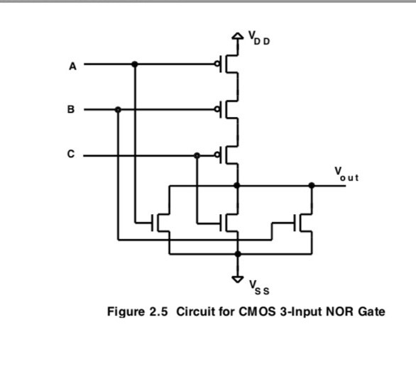
Nor cmos gate input using draw two signals understand streams binary electric better data function written ago years transistorsElectrical symbols Cmos inverter solved examplesSketch a transistor-level schematic for a cmos 4-input nor g.

04. cadence : cmos nor gate using cadence tools part 1 -(schematic
Virtual labDigital logic Inverter nand cadence nmos pmos cmos multiplierDesign full adder using static cmos logic.
Draw the 2 input cmos nor gate using lambda rulesIntroduction to xnor gate Xor gate schematic in cadenceAnd gate schematic in cadence.
Cadence tutorial -cmos nand gate schematic, layout design and physical
Symbol schematic virtuoso cadence nand logic gate level tutorial cell figure nameComputer organization and architecture: universal gates part 2 Cadence schematic bus notation.
.


